 手机:17359299796
— 产品中心 —
 全国免费客服电话 17359299796
 邮箱:A3669372910@163.com
手机:17359299796
电话:17359299796
地址:福建省漳州市龙文区朝阳北路1号办公楼205室
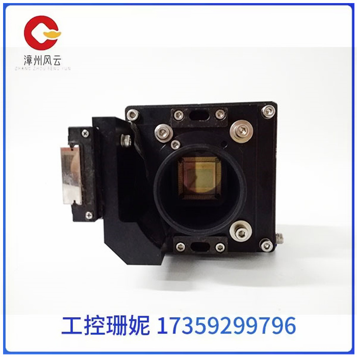
BASLER A404K 摄像机 A400系列单色颜色 3.54英寸品牌BASLER产品名称摄像机电压额定电流BASLER A404K 摄像机频率BASLER A404K适用行业铝业适用行业1运输业适用行业2石油最小包装1是否进口否适用行业3摄影可售卖地全国BASLER A404K 摄像机 A400系列单色颜色 3.54英寸工业相机是机器视觉系统中最关键的组件之一,其将光信号转变为有序的电信号,可
产品详情
BASLER A404K 摄像机 A400系列单色颜色 3.54英寸
BASLER A404K 摄像机 A400系列单色颜色 3.54英寸
工业相机是机器视觉系统中最关键的组件之一,其将光信号转变为有序的电信号,可按照数据传送方式分为ccd/cmos,也可按结构特性分为线阵/面阵等;选型时主要取决于使用场景、分辨率、帧率等因素,结合像元大小、靶面尺寸等参数完成,是影响图像质量最直接的因素。
一、芯片类型
一般来说,工业相机可按照芯片类型分为CCD和CMOS两种,这里我们分别展开介绍。
在感光元件受到光照后,将光信号转化为电信号,产生大小与光强相对应的电流(模拟信号)。在CCD传感器中,每一个感光元件都不对此作进一步的处理,而是将它直接输出到垂直寄存器,传到水平寄存器中,最后经一个放大器放大后统一输出(由于感光元件生成的电信号实在太微弱且存在电压损耗,无法直接进行模数转换工作,因此这些输出数据必须做统一的放大处理—这项任务是由CCD传感器中的放大器专门负责)。经放大器处理之后,每个像点的电信号强度都获得同样幅度的增大(因信号均通过一个放大器进行放大,所以产生的噪点较少)。后通过模数转换芯片转为数字信号,最终以二进制数字图像矩阵的形式输出给专门的DSP处理芯片。
相对于CCD的工作方式,CMOS传感器中每一个感光元件都直接整合了放大器和模数转换逻辑,当感光二极管接受光照、产生模拟的电信号之后,电信号首先被该感光元件中的放大器放大,然后直接转换成对应的数字信号。换句话说,在CMOS传感器中,每一个感光元件都可产生最终的数字输出,所得数字信号合并之后被直接送交DSP芯片处理。由于放大器属于模拟器件,因此很难保证每个像点的放大率都保持严格一致,导致放大后的图像数据无法代表拍摄物体的原貌体现在最终的输出结果上,使得品质明显低于CCD传感器,不过目前这方面的技术已大幅改善。

BASLER A404K 摄像机 A400系列单色颜色 3.54英寸
The industrial camera is one of the most critical components in the machine vision system, which converts the optical signal into an ordered electrical signal, which can be divided into ccd/cmos according to the data transmission mode, and can also be divided into linear array/surface array according to the structural characteristics; Selection mainly depends on the use of the scene, resolution, frame rate and other factors, combined with pixel size, target size and other parameters to complete, is the most direct factor affecting the image quality.
1. Chip type
In general, industrial cameras can be divided into CCD and CMOS according to the chip type, here we separately introduced.
After the sensor is illuminated, the light signal is converted into an electrical signal, and the size of the current corresponding to the light intensity is generated (analog signal). In the CCD sensor, each sensor is not further processed, but it is directly output to the vertical register, transmitted to the horizontal register, and finally unified output after amplification by an amplifier (because the electrical signal generated by the sensor is too weak and there is voltage loss, can not be directly carried out analog-to-digital conversion work, Therefore, these output data must be uniformly amplified - this task is exclusively handled by the amplifier in the CCD sensor). After being processed by the amplifier, the strength of the electrical signal at each image point is increased by the same amplitude (because the signal is amplified by one amplifier, less noise is generated). Then it is converted into digital signal by analog-to-digital conversion chip, and finally output to special DSP processing chip in the form of binary digital image matrix.
Relative to the working mode of CCD, each photosensitive element in CMOS sensor directly integrates the amplifier and analog-to-digital conversion logic, when the photosensitive diode receives light and generates an analog electrical signal, the electrical signal is first amplified by the amplifier in the photosensitive element, and then directly converted into the corresponding digital signal. In other words, in a CMOS sensor, each sensor can produce a final digital output, and the resulting digital signal is combined and sent directly to the DSP chip for processing. Because the amplifier belongs to the simulator, it is difficult to ensure that the magnification of each image point is strictly consistent, resulting in the amplified image data can not represent the original appearance of the shot object reflected in the final output result, making the quality significantly lower than the CCD sensor, but the current technology in this area has been greatly improved.
相关推荐